FWD Skill Zone
  • home
  • Power
    • Breadboard Power Supply
    • Variable Power Supply
    • DC to DC Boost Converter
  • Robotics
    • Braccio Robotic Arm
    • Voice-activated robotic arm
    • Smart Robot Car
  • Electronics
    • Arduino 101
    • Arduino 102
    • Arduino 103
    • Short Range Radar System
  • 3D print
  • VHDL
    • Intro to VHDL
    • 2 to 4 Binary Decoder
    • 3 to 8 Binary Decoder
    • Universal Shift Register
  • Verilog
    • Intro to Verilog
    • Verilog Construction
    • Verilog Examples
  • Machine Learning
    • Deep Learning
    • Transfer Learning
  • Contact us

​VHDL - Programming the Field Programmable Gate Array (FPGA)

Universal Shift Register

In this tutorial, we will design and implement a 4-bit universal shift register that can perform right shift, left shift, and parallel loading. Universal Shift Register is a register which can be arranged to load and retrieve the data in different mode of operation. 
Likewise, a universal shift register is a combined design of serial in serial out (SISO), serial in parallel out (SIPO), parallel in serial out (PISO) , and parallel in parallel out (PIPO.)
This project requires four D flip-flops and four 4-to-1 multiplexers. We will also use component instantiating method and structural VHDL coding in Xilinx .
Picture
Universal Shift Register Block diagram
​For this tutorial, we will be using a pre-designed D flip flop and 4 to 1 mux VHDL design codes. Then we will instantiate the components as requires to achieve the desired design out puts.​​​
\(\color{red}{Note:}\) make sure you save the D flip flop and 4 to 1 mux in the same directory as the Universal Shift Register.
As it is shown in the block diagram above, the design will have serial inputs, mode selector, parallel inputs, clock, clear signals, and output. We will also use multiplexers so that the register can perform left shifting, right shifting, and parallel loading depending on the selection on the multiplexer. 
Multiplexer M[0:1]
 00   No change
 01   Shift right (Input -> Q3, Q3->Q2, Q2->Q1, Q1->Q0)
 10   Shift left (Q3 <- Q2, Q2 <- Q1, Q1 <-Q0, Q0 <- Input)
 11  Parallel Load (P3 ->Q3, P2 ->Q2, P1 -> Q1, P0 -> Q0)
M(1)
M(0)
Operation
'0'
'0'
do nothing
'0'
'1'
shift right
'1'
'0'
shift left
'1'
'1'
parallel load
First, write a VHDL behavioral code for the D flip flop and multiplexer module using behavioral abstract techniques.
\(\color{red}{Note:}\) don't forget to write VHDL code the D flip flop and 4 to 1 mux and save them in the same directory as the D-FF and Mux combined Module and Universal Shift Register (VHDL code shown below).

 1. D-Flip-Flop with Asynchronous Reset
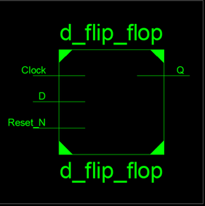
Design the model of the D-flip-flop as shown in the code below. In order to model the asynchronous behavior of the "reset" signal, add reset and clock in the sensitivity list of the "process" block. The clock and reset signals are now used to trigger the process. The if/elsif statement checks if the reset input has been asserted. If it is asserted, then it makes the appropriate assignments to the output, Q. ​If the reset has not been asserted, the elsif clause checks if a rising edge of the clock has occurred. If it is, the outputs are updated accordingly (Q <= D, Qn <= ~ D). The VHDL code below shows the behavioral model for a rising edge triggered D-flip-flop with an asynchronous reset.
library IEEE;
use IEEE.STD_LOGIC_1164.ALL;

entity d_flip_flop is
    Port ( D : in  STD_LOGIC;
           Clock : in  STD_LOGIC;
           Reset_N : in  STD_LOGIC;
           Q : out  STD_LOGIC);
end d_flip_flop;

architecture Behavioral of d_flip_flop is

begin
	process (Reset_N, Clock)
	Begin
		if Reset_N = '0' then
			Q <= '0';
		elsif Clock'EVENT AND Clock = '1' then
			Q<= D;
		end if;
	end process;
end Behavioral;
Picture

2. Multiplexer (4 to 1 mux)
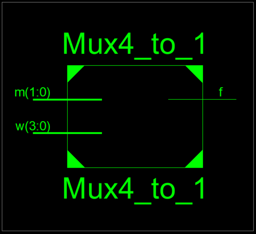
A multiplexer is a circuit that passes one of its multiple inputs to an output based on a select input m[0:1]. This can be The VHDL code below shows the process of designing a 4-to-1 multiplexer using behavioral modeling technique. 
library IEEE;
use IEEE.STD_LOGIC_1164.ALL;

entity Mux4_to_1 is
 Port ( w : in  STD_LOGIC_VECTOR (3 downto 0);
		  m : in  STD_LOGIC_VECTOR (1 downto 0);
		  f : out  STD_LOGIC);
end Mux4_to_1;

architecture Behavioral of Mux4_to_1 is

begin
	with m select
	f <= 	w(0)	when "00",
			w(1)	when "01",
			w(2) 	when "10",
			w(3) 	when others;
end Behavioral;
Picture

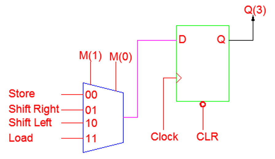
3. D-Flip-Flop and Mux 
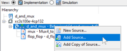
Then, write a VHDL structural code for the D flip flop and multiplexer module by using the previously designed D flip flop & multiplexer.
Picture
D flip flop and multiplexer module

4. D-FF and Mux VHDL code 
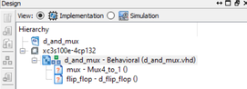
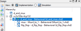
library IEEE;
use IEEE.STD_LOGIC_1164.ALL;

entity d_and_mux is
 Port ( in_put : in  STD_LOGIC_VECTOR (3 downto 0);
		  Sel : in  STD_LOGIC_VECTOR (1 downto 0);
		  clk :	in STD_LOGIC;
		  clearN : in STD_LOGIC;
		  Outp : out  STD_LOGIC);
end d_and_mux;

architecture Behavioral of d_and_mux is
	component Mux4_to_1
	Port ( w : in  STD_LOGIC_VECTOR (3 downto 0);
			 m : in  STD_LOGIC_VECTOR (1 downto 0);
			 f : out  STD_LOGIC);
	end component;

	component d_flip_flop
	Port ( D : in  STD_LOGIC;
			 Clock : in  STD_LOGIC;
			 Reset_N : in  STD_LOGIC;
			 Q : out  STD_LOGIC);
	end component;

signal mux_d : STD_LOGIC;

begin
	mux:	Mux4_to_1	PORT MAP (
	w=>in_put,  m=> Sel, f=> mux_d);
	flip_flop:  d_flip_flop	PORT MAP ( 
	D=>mux_d, Q=>Outp, Clock=>clk,  Reset_N => clearN
	);
end Behavioral;

If you see red error symbol "?" inside the hierarchy pane of the design panel, it is warning you that the instantiating black box module is missing
Picture
To fix this error, right click on the module "d_and_mux" and select "add Source" and locate the VHDL code, "Mux4_to_1.vhd"  that we created at step 2 above. Do the same thing for "d_flip_flop".
Picture
Save the module and now the error should go away as shown below.
Picture

5. Universal Shift Register VHDL code

Next, write a VHDL structural code for the Universal Shift Register by instantiating the combined D flip flops and Multiplexers modules (d_and_mux) using the component port map statements.
Picture
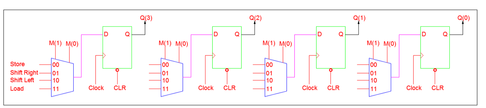
Universal Shift Register schematics
library IEEE;
use IEEE.STD_LOGIC_1164.ALL;

entity uni_shift_reg is
    Port ( input : in  STD_LOGIC;
           load : in  STD_LOGIC_VECTOR (3 downto 0);
           outp : out  STD_LOGIC_VECTOR (3 downto 0);
			  clk_1 : in  STD_LOGIC;
           sel : in  STD_LOGIC_VECTOR (1 downto 0);
           clr_1 : in  STD_LOGIC);
end uni_shift_reg;

architecture Behavioral of uni_shift_reg is
	component d_and_mux
	Port ( in_put : in  STD_LOGIC_VECTOR (3 downto 0);
           Sel : in  STD_LOGIC_VECTOR (1 downto 0);
			  clk :	in STD_LOGIC;
			  clearN : in STD_LOGIC;
           Outp : out  STD_LOGIC);		
	end component;
	signal sh_left: STD_LOGIC_VECTOR (2 downto 0);
	signal sh_right: STD_LOGIC_VECTOR (3 downto 0);
	signal store: STD_LOGIC_VECTOR (3 downto 0);
begin
	Stage3: d_and_mux  
	PORT MAP (in_put(0) => store(3),
		  in_put(1) =>	input,
		  in_put(2) => sh_left(2),
		  in_put(3) =>	load(3), 
		  clk => clk_1, 
		  Sel => sel, 
		  clearN => clr_1, 
		  OutP => sh_right(3));
										  
										  
	Stage2: d_and_mux  
	PORT MAP (in_put(0) => store(2), 
		  in_put(1) =>	sh_right(3),
		  in_put(2) => sh_left(1),
		  in_put(3) =>	load(2), 
		  clk => clk_1, 
		  Sel => sel, 
		  clearN => clr_1, 
		  OutP => sh_right(2));
										  
	Stage1: d_and_mux  
	PORT MAP (in_put(0) => store(1), 
		  in_put(1) =>	sh_right(2),
		  in_put(2) => sh_left(0),
		  in_put(3) =>	load(1), 
		  clk => clk_1, 
		  Sel => sel, 
		  clearN => clr_1, 
		  OutP => sh_right(1));
										  
										  
	Stage0: d_and_mux  
	PORT MAP (in_put(0) => store(0), 
		  in_put(1) =>	sh_right(1),
		  in_put(2) => input,
		  in_put(3) =>	load(0), 
		  clk => clk_1, 
		  Sel => sel, 
		  clearN => clr_1, 
		  OutP => sh_right(0));
			
		
	outp(3) <= sh_right(3);
	store(3) <= sh_right(3);
	
	outp(2) <= sh_right(2);
	store(2) <= sh_right(2);
	sh_left(2) <= sh_right(2);
	
	outp(1) <= sh_right(1);
	store(1) <= sh_right(1);
	sh_left(1) <= sh_right(1);
	
	outp(0) <= sh_right(0);
	store(0) <= sh_right(0);
	sh_left(0) <= sh_right(0);

end Behavioral;


6. Test Bench
The functionality of the VHDL designs is verified through a simulation using a test bench. A test bench is a VHDL system that instantiates the system to be tested (the system being tested is often called a Device Under Test (DUT) or Unit Under Test (UUT)) and then simulates the input parameters and displays the outputs as a waveform.
LIBRARY ieee;
USE ieee.std_logic_1164.ALL;
 
ENTITY Uni_shift_reg_TB IS
END Uni_shift_reg_TB;
 
ARCHITECTURE behavior OF Uni_shift_reg_TB IS 
 
    -- Component Declaration for the Unit Under Test (UUT)
 
    COMPONENT uni_shift_reg
    PORT(
         input : IN  std_logic;
         load : IN  std_logic_vector(3 downto 0);
         outp : OUT  std_logic_vector(3 downto 0);
         clk_1 : IN  std_logic;
         sel : IN  std_logic_vector(1 downto 0);
         clr_1 : IN  std_logic
        );
    END COMPONENT;
	 
   --Inputs
   signal input : std_logic := '0';
   signal load : std_logic_vector(3 downto 0) := (others => '0');
   signal clk_1 : std_logic := '0';
   signal sel : std_logic_vector(1 downto 0) := (others => '0');
   signal clr_1 : std_logic := '0';

 	--Outputs
   signal outp : std_logic_vector(3 downto 0);

   -- Clock period definitions
   constant clk_1_period : time := 10 ns;
 
BEGIN
 
	-- Instantiate the Unit Under Test (UUT)
   uut: uni_shift_reg PORT MAP (
          input => input,
          load => load,
          outp => outp,
          clk_1 => clk_1,
          sel => sel,
          clr_1 => clr_1
        );

   -- Clock process definitions
   clk_1_process :process
   begin
		clk_1 <= '0';
		wait for clk_1_period/2;
		clk_1 <= '1';
		wait for clk_1_period/2;
   end process;
 
   -- Stimulus process
   stim_proc: process
   begin		
      -- test CLR 
		clr_1<='0'; 
		wait for 30ns; 
		-- test parallel loading 
		clr_1<='1'; 
		sel<="11"; 
		load<="0110"; 
		wait for 40ns; 
		-- test shift right 
		sel<="01"; 
		input<='1'; 
		wait for 80ns; -- shift 4 bits 
		-- test shift left 
		sel<="10"; 
		input<='0'; 
		wait for 80ns; -- shift 4 bits 
		wait; 

   end process;

END;

Next, simulate the testbench code and obtain a wave form similar to the one shown below. Don't forget to adjust the simulation run time to at least 200ns to allow the testbench code goes through all the possible combinations of the inputs. 
Picture
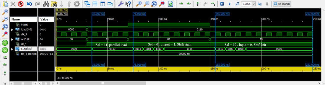
Waveform for Universal Shift Register.

PORT mapping for Basys FPGA ​
User Constraint File (UCF) for ​- Basys 2 FPGA Board
​# PlanAhead Generated physical constraints
NET "clk_1" CLOCK_DEDICATED_ROUTE = FALSE;
NET "load[3]" LOC = B4;
NET "load[2]" LOC = K3;
NET "load[1]" LOC = L3;
NET "load[0]" LOC = P11;
NET "outp[3]" LOC = P6;
NET "outp[2]" LOC = P7;
NET "outp[1]" LOC = M11;
NET "outp[0]" LOC = M5;
NET "sel[1]" LOC = E2;
NET "sel[0]" LOC = F3;
NET "clk_1" LOC = G12;
NET "clr_1" LOC = N3;
NET "input" LOC = G3;

​


Finally, generate a programming file (.bit), Connect the FPGA board to the computer and program the FPGA board using the ADEPT software. ​
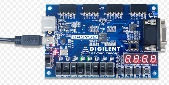
Picture
For more information visit:
​ ​Basys 2 Reference Manual

Back << 3 to 8 Decoder

      ​


PAGE TAGS AutoCAD CAD CATIA Digital Logic Matlab VHDL Links Programming VHDL Verilog Xilinx AMD

  • home
  • Power
    • Breadboard Power Supply
    • Variable Power Supply
    • DC to DC Boost Converter
  • Robotics
    • Braccio Robotic Arm
    • Voice-activated robotic arm
    • Smart Robot Car
  • Electronics
    • Arduino 101
    • Arduino 102
    • Arduino 103
    • Short Range Radar System
  • 3D print
  • VHDL
    • Intro to VHDL
    • 2 to 4 Binary Decoder
    • 3 to 8 Binary Decoder
    • Universal Shift Register
  • Verilog
    • Intro to Verilog
    • Verilog Construction
    • Verilog Examples
  • Machine Learning
    • Deep Learning
    • Transfer Learning
  • Contact us