Dual-Polarity-Variable Linear Power Supply [DPV-LPS]
Disclaimers:
Objectives:
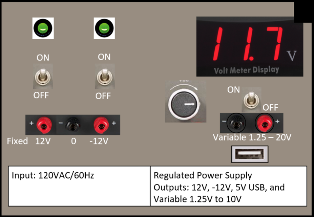
The goal of this project is to design and build a Dual-Polarity-Variable Linear Power Supply with an external 5-Volt Universal Serial Bus (USB) port, fixed ±12V, and a variable 1.25V to 10V output at a maximum current of 1A. Theory: The theory behind designing this DPV-LPS consists of using a transformer to step down the 120 VAC input to a 24 VAC, followed by a full-bridge rectifier composed of four diodes that convert the AC voltage into a pulsating DC. Then, using capacitor(s) the pulsating Direct Current is converted into a pure Direct Current. The output filter capacitors smooth out the ripple in the DC output. Finally, voltage regulators are used to obtain different voltage outputs and to automatically maintain a constant voltage level at the output. 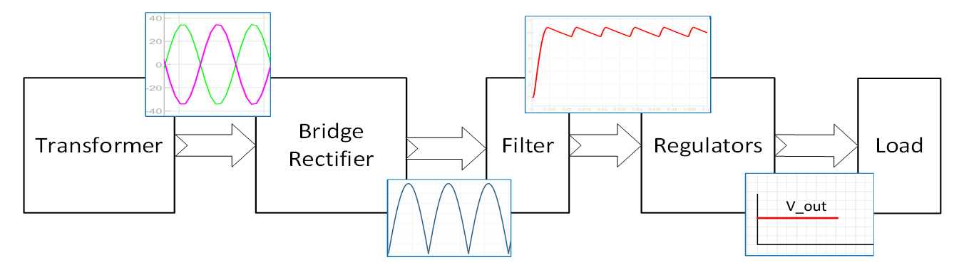
Major components:
Transformer: To step down 120V to 24V The transformer plays a key role in the design of the DC power supply. This design uses a center-tap, step down transformer that decreases a 120V coming from a wall outlet down to a 24V with a maximum current of 1A. This type of transformer is called center-tap because the two outer taps (total winding) of the transformer gives the total voltage across the transformer, and half of the total voltage is measured from each outer tap to the center terminal. For example, the voltage across the two outer taps (winding as a whole) of the transformer that is used for this project is 24 VAC, and it provides 12VAC from each outer tap to the center tap (half winding). These two 12VAC supplies are 180 degrees out of phase with each other; therefore, it is easy to derive the positive and the negative 12-volt requirements. 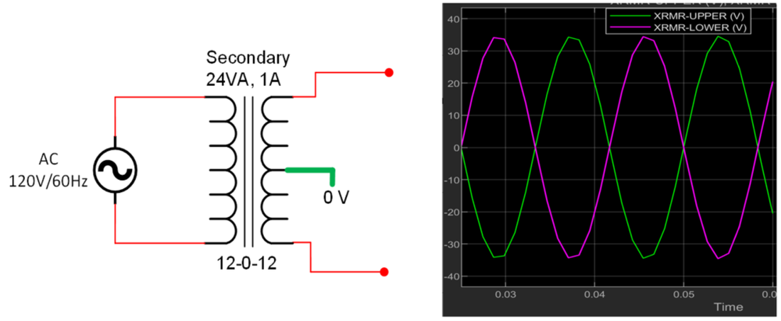
Center Tap XFMR and output waveforms
For the center-tapped transformer shown above, the output is a sine wave centered around zero volt. The peak voltage Vpk is 1.414 (square root of 2) times the RMS output of the transformer. Then, for a 120V:24V transformer the peak voltage will be 1.414 times 24 = 33.94V across the outer ends of the transformer. The transformer will also have losses at the windings; however, a transformer rated at 120V: 24V at 1A will usually provide more than 30V RMS output. Therefore, this transformer is ideal for this project as the voltage output will be higher than what we need.
Rectifier: To convert AC to DC AC to DC conversion requires the use of a transformer and rectifier as shown in figure below. The transformer steps the voltage up or down based on the requirements; and the rectifier removes the negative cycle of the input signal, resulting in only positive voltage output. The diagram below shows a bridge rectifier fed from a center tap transformer. 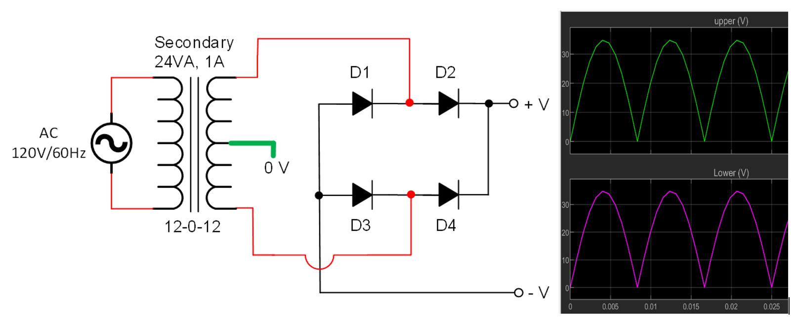
Center Tap XFMR and Bridge Rectifier (unfiltered) and output waveforms
Filter or Smoothing capacitor(s): To reduce the amount of AC ripple on the DC voltage As it is discussed above, the output from the transformer/rectifier circuit is a pulsating DC voltage that contains a large unwanted AC component. A rectifier circuit without a filter produces pulsating output. This fluctuation can be reduced if some of the energy can be stored in a capacitor while the rectifier is producing pulses and if it is allowed to discharge the capacitor between pulses. This is where the use of the filter capacitor comes into the picture. The capacitor that is installed in parallel with the load resistor reduces the pulsating action of the rectifier output wave. Then, the filter capacitor charges rapidly and discharges slowly; as a result, it will smooth the waveform. 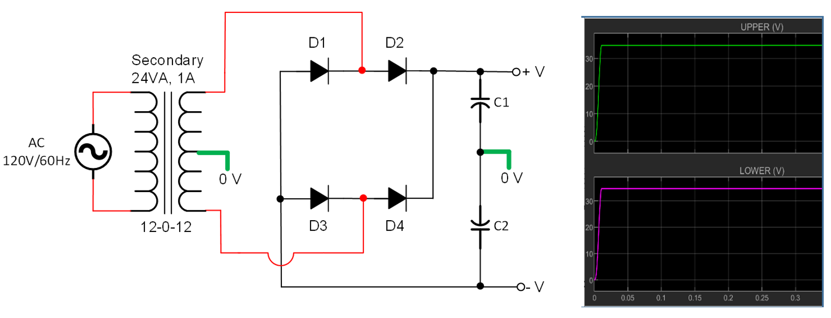
Bridge Rectifier (filtered) and output waveforms
Voltage regulators: To provide a regulated output voltage The regulator section of the power supply controls the output voltage level to a constant value irrespective of the input voltage, load, or temperature variations. The voltage regulators maintain a constant voltage level regardless of the fluctuation of the input voltage. Depending on the design, a regulator may be used to provide the desired output voltage. This voltage regulator can use either a simple forward, or a negative feedback design. For this project, the following three types of voltage regulators are used: LM7912, LM7812 and LM317. The LM78XX and LM79XX are three-terminal regulators with TO-220 through-hole package. These regulators have fixed output voltages, making them useful in a wide range of applications. According to the datasheet, these voltage regulators have internal current limiting, thermal shut-down, and safe area protection circuits. Besides, with appropriate heat sink, they can provide regulated voltages with over 1A output current. Similarly, the LM317 voltage regulator comes in TO-220 packages and it is intended for use as positive adjustable voltage regulators. LM317 can provide more than 1.5 A of load current with an output voltage adjustable over a range of 1.2V to 37 V. The desired output voltage is determined by means of a resistive voltage divider circuit. This makes LM317 remarkably easy to use device for any output in the range of 1.25 to 37V. To get the required output voltage, we need only two resistors or a resistor and a potentiometer. Note: refer to the respective datasheets for detail information. According to the datasheet, the output of the LM317 voltage regulator is determined by the following formula:
Circuit Diagram
After collecting all the required information and calculation results, the power supply circuit is designed as shown below. This circuit diagram has additional components that were not discussed above. These components are not mandatory to the design, but they will enhance the fit-form-function of the DPV-LPS. Besides, the reverse current protection diodes and the STSP switches are also added as additional safety features. 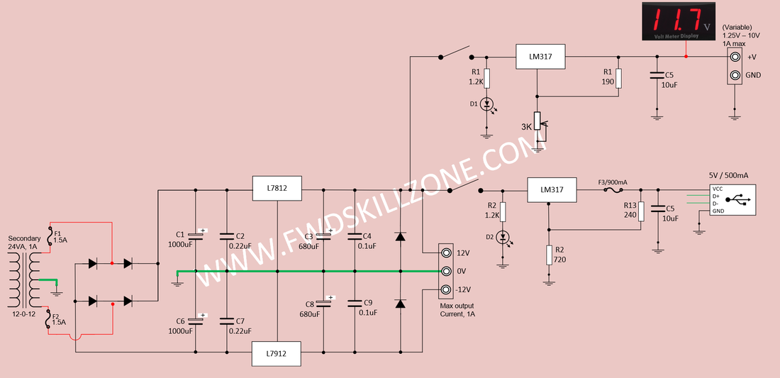
Circuit diagram of the DPV-LPS
DC Analysis:
The following analysis of the +12V and -12V output is performed in OrCAD capture simulation program. The power supply is analyzed without a load as shown in the figure below. Here, we are testing the two voltage regulator outputs, LM7912, and LM7812 without a load. As it is shown in figure below, regulator #1 is providing +12.801V at no load and regulator #2 is providing -12.428V. 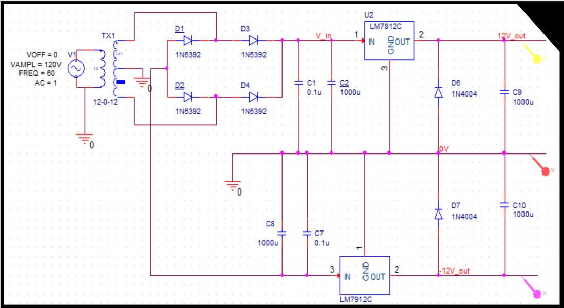
OrCAD simulation of the DPV-LPS at no-load.
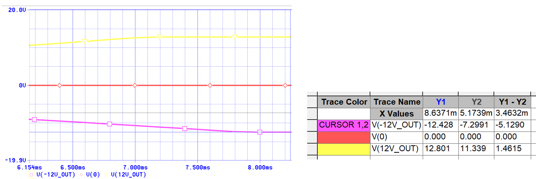
Waveform and cursor values of the no-load simulation
Voltage Regulation:
Voltage regulation is the measure of how well our power supply maintains constant output voltage over a range of loads. Voltage regulation is calculated using the following formula: \(\color{blue}{V_{reg} = \frac {V_{NL} - V_{FL}} {V_{FL}}*100% }\) Printed Circuit Board
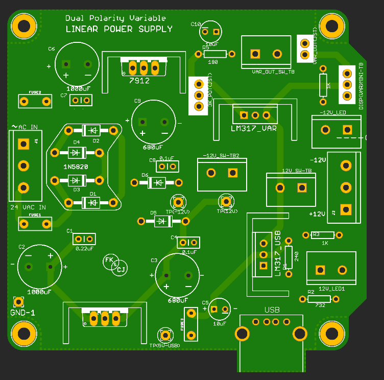
The Printed Circuit Board (PCB) of the DPV-LPS is designed in Eagle CAD program. Note: EagleCAD can be downloaded from the Autodesk website with a student e-mail address. The program helps the designer to connect schematic diagrams, component layout, PCB circuit routing, and component library. The free version of Eagle CAD has a limitation of only two schematic sheets, double layers, and an 80 cm^2 board area. However, for a small project like this one, these limitations are not big deals. The PCB design is started in the “schematic” workbench of the Eagle CAD program and all the symbols for the components are placed and oriented on a blank schematic sheet as shown in figure below. 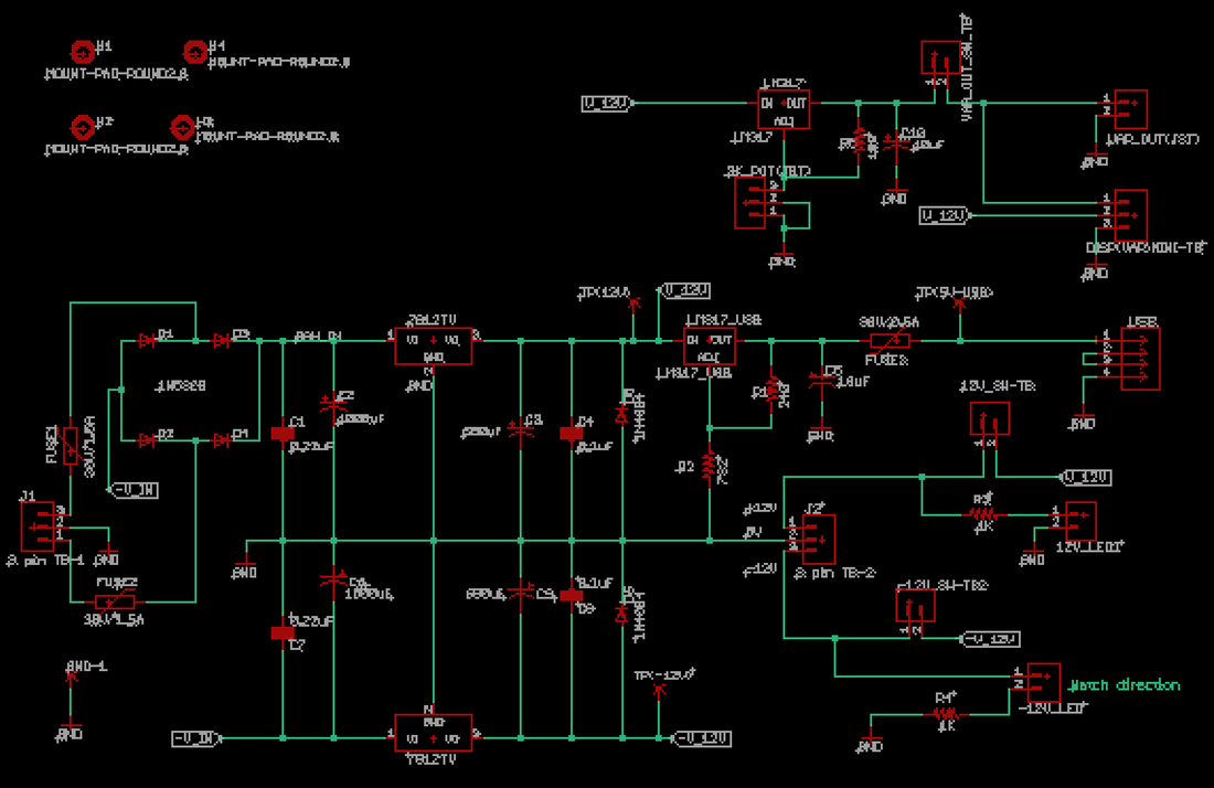
EagleCAD PCB schematic design
After the schematic is done, next, electrical connectivity is made between each part with “nets” layer and assigned values and names to our parts accordingly. Finally, we make sure everything is connected as per the Eagle CAD design criteria by running an Electrical Rule Check (ERC). Then, the board layout is done on the “board” workbench of Eagle CAD. Then we used a “PCB Trace Width Calculator” tool to calculate the race width and routed the corresponding wires with an appropriate trace width of 65 mils. Then, a copper pour of the ground plane is created on both top & bottom layers of the PCB and connected these ground planes with multiple “vias” to connect the two opposite layers of the board. These “vias” also help reduce heat resistance of the copper pour across the PCB.
Next, perform Design Rule Check (DRC) to validate the “board” design meets the industry standards. Then, fix all the DRC errors until you get “DRC: No error” message. Finally, convert the file to a Gerber file format using the CAM Processor of the Eagle CAD and then send the Gerber file to a PCB fabrication company such as:
- PCB way - https://www.pcbway.com/ - OSH park - https://oshpark.com/ - JLC PCB - https://jlcpcb.com Once the PCB is fabricated, solder all the components onto the PCB as shown in the figure below. 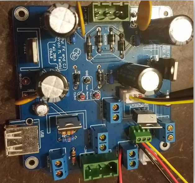
PCB component assembly
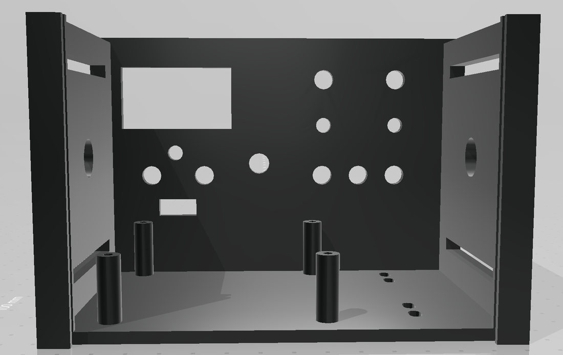
Next, design and manufacture an enclosure that is approximately is 150mm x 94mm x 100mm (L*W*H) and it should have four PCB mounting holes or standoffs with a hole diameter of 3mm and which are 70.23mm apart (center to center) horizontally and 70.10mm apart vertically. Then, connect all electrical wirings from the PCB to the enclosure.
In our case, we used a 3D printer to manufacture the enclosure as shown below.
Note: potentiometer mounting hole is relocated to a new position due to interference with other components. Functional Test
1. No-load test Finally, Perform successive output tests as shown the following table and calculate the percent error. Percent error is calculated using the formula: \(\color{blue}{Percent_{error} = (\frac {{Actual}-{Expected}}{Expected})*100 }\) 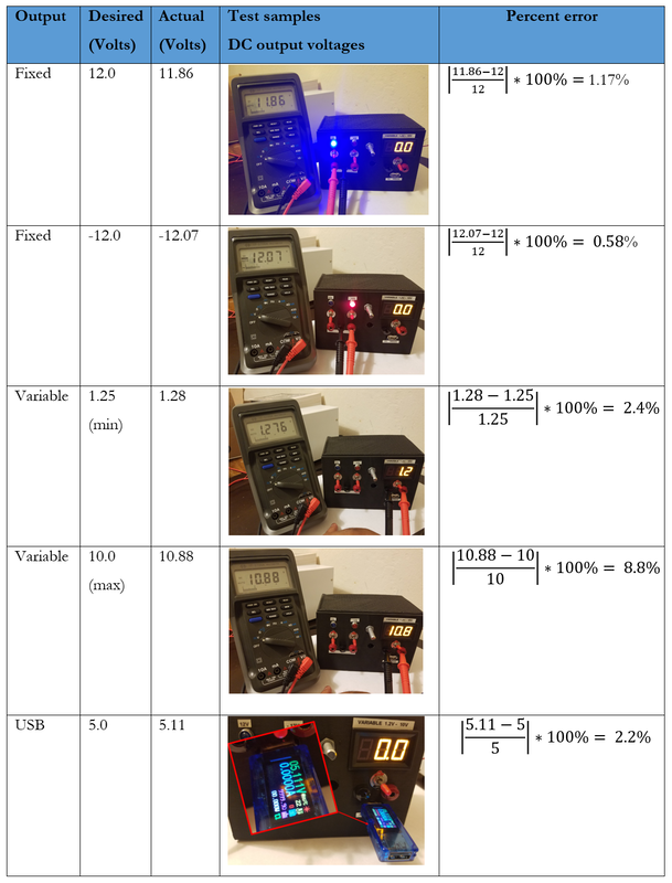
No-load output test
2. Output load test The following output test is performed to validate the maximum output current at different loads. While charging a tablet that has a fully drained battery, the maximum load current of 900 mA is obtained from the DPV-LPS as shown in the figure below. 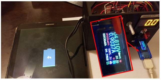
USB charging max output current test
Conclusion:
In this project, we have seen the design and build processes for a Dual-Polarity-Variable Linear Power Supply that provides fixed 12V and -12V, 5V (USB), and a variable 1.25V to 10V outputs. The design of the DPV-LPS consists of a transformer to step down the 120 VAC input to a 24 VAC followed by a full-bridge rectifier composed of four diodes that convert the AC voltage into DC voltage. Then, using capacitor(s), the pulsating Direct Current is converted into pure Direct Current. The filter capacitors smooth out the ripple in the DC output. Finally, voltage regulators are used to obtain different voltage outputs and to automatically maintain a constant voltage level at the output. »»» END of DPV-LPS Design »»» Have a question, comments, or need the EagleCAD file? - click here to contact us |
|