FWD Skill Zone
  • home
  • Power
    • Breadboard Power Supply
    • Variable Power Supply
    • DC to DC Boost Converter
  • Robotics
    • Braccio Robotic Arm
    • Voice-activated robotic arm
    • Smart Robot Car
  • Electronics
    • Arduino 101
    • Arduino 102
    • Arduino 103
    • Short Range Radar System
  • 3D print
  • VHDL
    • Intro to VHDL
    • 2 to 4 Binary Decoder
    • 3 to 8 Binary Decoder
    • Universal Shift Register
  • Verilog
    • Intro to Verilog
    • Verilog Construction
    • Verilog Examples
  • Machine Learning
    • Deep Learning
    • Transfer Learning
  • Contact us

​VHDL - Programming the Field Programmable Gate Array (FPGA)

3 to 8 Binary Decoder VHDL Design​

In this tutorial, we will design and implement a 3-to-8 decoder using two 2-to-4 decoders in Xilinx ISE CAD tool. The implementation will be on Basys 2 FPGA  board using VHDL programming language. ​
V - VHSIC: Very High Speed Integrated Circuit
H - Hardware
D- Description
​L - Language
Note: make sure you save the 2-to-4 component in the same directory with the 3-to-8 decoder in work.

          Truth table for 3 to 8 Decoder ​

Picture

3 to 8 Decoder VHDL Structural Code 

library IEEE;
use IEEE.STD_LOGIC_1164.ALL;
use IEEE.STD_LOGIC_ARITH.ALL;
entity dec3_to_8 is
  Port ( enable : in  STD_LOGIC;
       w : in  STD_LOGIC_VECTOR (2 downto 0);
       y : out  STD_LOGIC_VECTOR (7 downto 0));
end dec3_to_8;
architecture structure of dec3_to_8 is
  component dec2to4
     port (enable : in  STD_LOGIC;
     sw : in  STD_LOGIC_VECTOR (1 downto 0);
     led : out  STD_LOGIC_VECTOR (3 downto 0));
  end component;
            signal sig_1: STD_LOGIC;
            signal sig_2: STD_LOGIC;
            signal w_not: STD_LOGIC;
begin
 stage1: dec2to4          
 PORT MAP (
   enable => sig_1,
    sw(0) => w(0),
    sw(1) => w(1),
    led(0)=> y(0),
    led (1) => y(1),
    led (2) => y(2),
    led (3) => y(3) );
​

 stage2: dec2to4          
 PORT MAP (
   enable => sig_2,
    sw(0) => w(0),
    sw(1) => w(1),
    led(0)=> y(4),
    led (1) => y(5),
    led (2) => y(6),
    led (3) => y(7));
    w_not <= NOT w(2);
    sig_1 <= w_not AND enable;
    sig_2 <= w(2) AND enable;      
end structure;
Once the structural code is checked for syntax error; then, create a test bench containing all input possibilities to validate the proper functionality of the VHDL code as well as the complete circuit design. Here, we  will modify the default test bench code as it has  clock signals; however, this design does not require the clock input. Therefore, remove all the codes that contains clock signal.​

3 to 8 Decoder Test bench ​

LIBRARY ieee;
USE ieee.std_logic_1164.ALL;
use IEEE.STD_LOGIC_ARITH.ALL;
use IEEE.STD_LOGIC_UNSIGNED.ALL;
ENTITY dec3_to_8_TB IS
END dec3_to_8_TB;
 ARCHITECTURE structure OF dec3_to_8_TB IS
   COMPONENT dec3_to_8
    PORT(
        enable : IN  std_logic;
        w : IN  std_logic_vector(2 downto 0);
        y : OUT  std_logic_vector(7 downto 0));
    END COMPONENT;
--Inputs
signal enable : std_logic := '0';
signal w : std_logic_vector(2 downto 0):=(others=> '0');
BEGIN
-- Instantiate the Unit Under Test (UUT)
   uut: dec3_to_8 PORT MAP (
          enable => enable,
          w => w,
          y => y);
-- Stimulus process
   stim_proc: process
   begin           
       wait for 100 ns;                       
           -- start test sequence
              w <= "000";
              enable <= '0';
           -- Test stage 1
              for index in 0 to 7 loop
                  wait for 100 ns;
                  w <= w + '1';
              end loop;
            -- Test stage 2            
                   w <= "000";
                   enable <= '1';
                   for index in 0 to 7 loop
                       wait for 100 ns;
                       w <= w + '1';
                   end loop;
                   wait;
   end process;
 END structure;

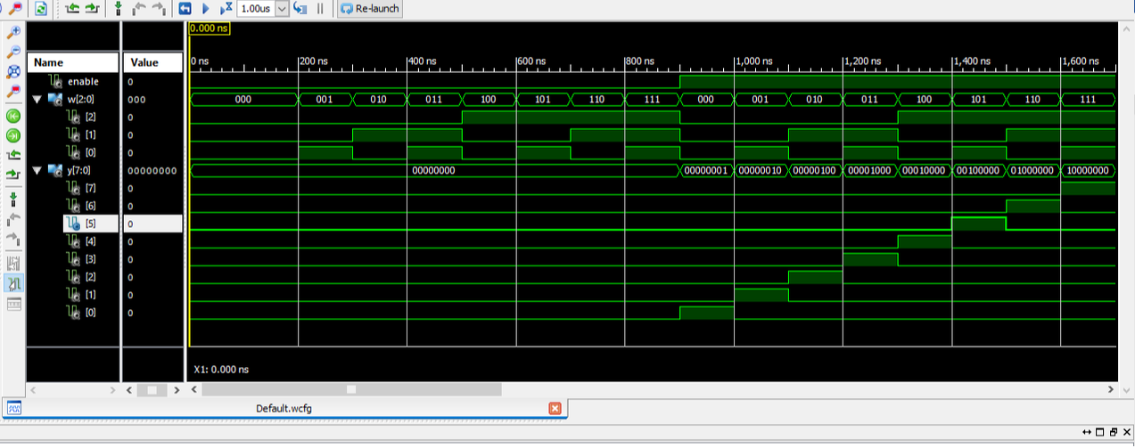
Then check the testbench code for syntax errors, and adjust the simulation run time to 100ns to allow the testbench code goes through all the possible combinations of the inputs. Next, run the simulation to obtain a waveform  similar to the figure shown below.

3 to 8 Decoder Waveform​
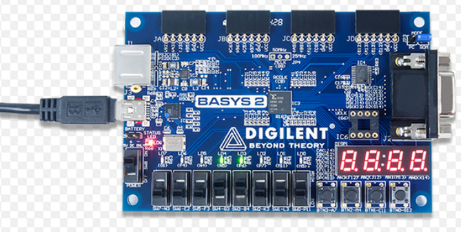
Picture

User Constraint File (UCF) for ​- Basys 2 FPGA Board

Create the implementation UCF file (.ucf) as shown bellow. This file contains the signal definitions and physical mapping of the pins on the Basys-2 FPGA board.

 
# PlanAhead Generated physical constraints
 NET "enable" LOC = N3;
NET "w[0]" LOC = P11;
NET "w[1]" LOC = L3;
NET "w[2]" LOC = K3;
NET "y[0]" LOC = M5;
NET "y[1]" LOC = M11;
NET "y[2]" LOC = P7;
NET "y[3]" LOC = P6;
NET "y[4]" LOC = N5;
NET "y[5]" LOC = N4;
NET "y[6]" LOC = P4;
NET "y[7]" LOC = G1;

Finally, generate a programming file (.bit), Connect the FPGA board to the computer and program the FPGA board using the ADEPT software. ​
Picture
For more information visit:
​ ​Basys 2 Reference Manual
Next  >>  Shift Register
Back  <<  2 to 4 Decoder

Next >> Shift Register
Back << 2 to 4 Decoder

PAGE TAGS AutoCAD CAD CATIA Digital Logic Matlab VHDL Links Programming VHDL Verilog Xilinx AMD

  • home
  • Power
    • Breadboard Power Supply
    • Variable Power Supply
    • DC to DC Boost Converter
  • Robotics
    • Braccio Robotic Arm
    • Voice-activated robotic arm
    • Smart Robot Car
  • Electronics
    • Arduino 101
    • Arduino 102
    • Arduino 103
    • Short Range Radar System
  • 3D print
  • VHDL
    • Intro to VHDL
    • 2 to 4 Binary Decoder
    • 3 to 8 Binary Decoder
    • Universal Shift Register
  • Verilog
    • Intro to Verilog
    • Verilog Construction
    • Verilog Examples
  • Machine Learning
    • Deep Learning
    • Transfer Learning
  • Contact us